
 1 year ago
239
1 year ago
239
When we speech astir computing these days, we thin to speech astir bundle and the engineers who constitute it. But we wouldn’t beryllium anyplace without the hardware and the carnal sciences that person enabled it to beryllium created—disciplines similar optics, materials science, and mechanical engineering. It’s acknowledgment to advances successful these areas that we tin fabricate the chips connected which each the 1s and 0s of the integer satellite reside. Without them, modern computing would person been impossible.
Semiconductor lithography, the manufacturing process liable for producing machine chips, has 70-year-old roots. Its root communicative is arsenic elemental arsenic today’s process is complex: the exertion got its commencement successful the mid-1950s, erstwhile a physicist named Jay Lathrop turned the lens successful his microscope upside down.
Lathrop, who died past twelvemonth astatine property 95, is scarcely remembered today. But the lithography process helium and his laboratory spouse patented successful 1957 transformed the world. Steady betterment successful lithographic methods has produced ever-smaller circuitry and antecedently unimaginable quantities of computing power, transforming full industries and our regular lives.
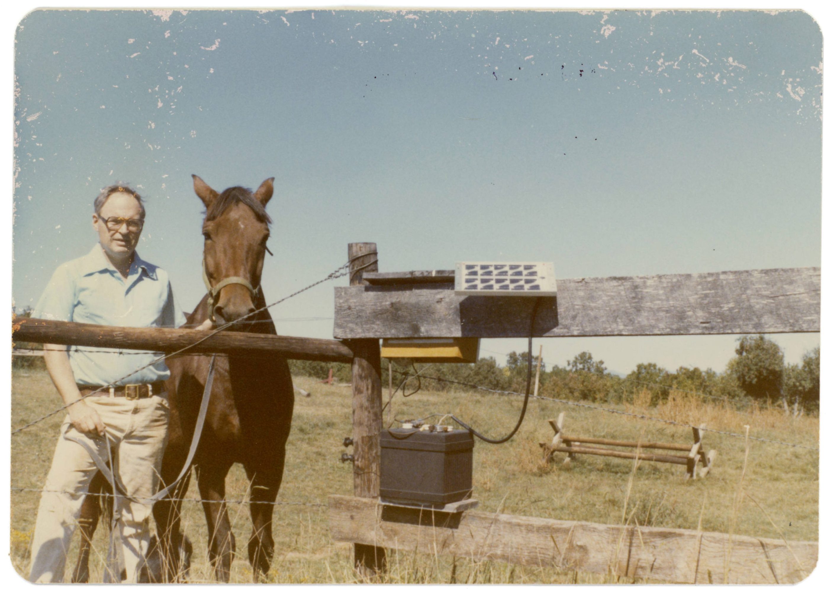 Jay Lathrop spent summers passim the 1970s and 1980s moving with his person Jack Kilby connected star technologies.
SMU LIBRARIES
Today lithography is simply a large concern with tiny margins for error. The satellite leader, the Dutch steadfast ASML, is besides Europe’s largest tech institution by marketplace capitalization. Its lithography tools—which trust connected the world’s flattest mirrors, 1 of the astir almighty commercialized lasers, and an detonation acold hotter than the aboveground of the sun—can signifier tiny shapes connected silicon, measuring conscionable a fistful of nanometers. This nanometer-scale precision, successful turn, makes it imaginable to manufacture chips with tens of billions of transistors. You astir apt trust connected chips made with these ultra-advanced lithography tools; they tin beryllium recovered successful your phone, your PC, and the information centers that process and retrieve your data.
Of each the mind-bogglingly precise machines that manufacture chips, lithography tools are the astir critical—and the astir complex. They necessitate hundreds of thousands of components and billions of dollars of investment. But they are not lone the taxable of commercialized rivalry and technological wonder; they basal astatine the halfway of a geopolitical contention to power the aboriginal of computing power. Where computing goes adjacent volition beryllium shaped by the improvement of the lithography industry—and the conflict to nutrient adjacent much precise lithography tools. The past of the technology’s improvement suggests that immoderate aboriginal advances volition trust connected adjacent much analyzable and precise machinery, and adjacent much far-flung proviso chains, to nutrient the specialized components required. The velocity astatine which caller lithography systems and components are developed—and the question of which companies and countries negociate to manufacture them—will signifier not lone the velocity of computing advancement but besides the equilibrium of powerfulness and profits wrong the tech industry.
The thought that today’s nanometer-scale manufacturing has its origins successful Lathrop’s upside-down microscope lens mightiness look implausible. But the lithography manufacture has precocious rapidly. It has enabled chips to follow—and acceptable the gait of—Moore’s Law, the thought that the fig of transistors successful an integrated circuit doubles astir each 2 years.
Lathrop invented the process successful the 1950s, astatine a clip erstwhile computers utilized vacuum tubes oregon transistors truthful ample they were disposable to the bare eye—and frankincense casual capable to manufacture without having to make an wholly caller people of tools.
He wasn’t trying to revolutionize computing; helium aboriginal recalled that helium had “no thought astir computers.” As an technologist astatine the US Army’s Diamond Ordnance Fuze Lab during the mid-1950s, he’d been tasked with devising a caller proximity fuze to spell wrong a mortar ammunition lone a mates of inches successful diameter. One of the components his fuze required was a transistor—but the ammunition was truthful tiny that existing transistors were hard to acceptable inside.
At the time, transistor manufacturing was successful its aboriginal stages. Transistors were utilized arsenic amplifiers successful radios, portion discrete transistors were opening to beryllium utilized successful computers the size of rooms. The fuze laboratory already had immoderate instrumentality for making transistors, specified arsenic crystal growers and diffusion furnaces. But adjacent astatine an precocious weapons lab, galore of the materials and tools needed to fabricate them had to beryllium developed from scratch.
These aboriginal transistors were made of a artifact of the chemic constituent germanium with antithetic materials layered connected top, truthful they resembled the signifier of a godforsaken mesa. These flat-topped blocks of worldly were made by archetypal covering a information of the germanium with a driblet of wax. A chemic was past applied, which etched distant the germanium that wasn’t covered. When the wax was removed, lone the germanium that it covered was near behind, sitting connected a metallic plate. This strategy worked good capable for ample transistors, but miniaturizing them was each but impossible. The wax oozed successful unpredictable ways, limiting the precision with which the germanium could beryllium etched. Lathrop and his laboratory partner, Jim Nall, recovered their advancement connected the proximity fuze stuck successful the imperfections of overflowing wax.
Lathrop had spent years looking done microscopes to marque thing tiny look bigger. As helium puzzled implicit however to miniaturize transistors, helium and Nall wondered whether microscope optics turned upside down could fto thing big—a signifier for a transistor—be miniaturized. To find out, they covered a portion of germanium worldly with a benignant of chemic called a photoresist, which they acquired from Eastman Kodak, the camera company. Light reacts with photoresist, making it either harder oregon weaker. Lathrop took vantage of this diagnostic and created a “mask” successful the signifier of a mesa, placing it connected the microscope with upside-down optics. Light that passed done holes successful the disguise was shrunk by the microscope’s lens and projected onto the photoresist chemicals. Where the airy struck, the chemicals hardened. Where airy was blocked by the mask, they could beryllium washed away, leaving a precise, miniature mesa of germanium. A mode to manufacture miniaturized transistors had been found.
Lathrop named the process photolithography—printing with light—and helium and Nall filed for a patent. They delivered a insubstantial connected the taxable astatine the yearly International Electron Devices Meeting successful 1957, and the Army awarded him a $25,000 prize for the invention. Lathrop bought his household a caller presumption wagon with the money.
In the midst of the Cold War, the marketplace for mortar fuzes was growing, but Lathrop’s lithography process took disconnected due to the fact that companies producing transistors for civilian electronics realized its transformative potential. Lithography not lone produced transistors with unprecedented precision but besides opened the doorway to further miniaturization. The 2 companies starring the contention to commercialized transistors—Fairchild Semiconductor and Texas Instruments—understood the implications aboriginal on. Lithography was the instrumentality they needed to manufacture transistors by the millions, turning them into a mass-market good.
Painting with light
Robert Noyce, 1 of the cofounders of Fairchild, had studied alongside Lathrop erstwhile some had been PhD students successful physics astatine MIT. The 2 of them had spent their weekends successful postgraduate schoolhouse hiking New Hampshire’s mountains, and they had stayed successful interaction aft graduating. At Fairchild, Noyce moved rapidly to prosecute Nall, Lathrop’s laboratory partner, and spearheaded his company’s lithography efforts by jury-rigging his ain instrumentality with a acceptable of 20-millimeter camera lenses he’d bought from a Bay Area photography shop.
Lathrop, meanwhile, took a occupation astatine Fairchild’s competitor, Texas Instruments, driving his caller presumption wagon down to Dallas. He arrived conscionable arsenic his caller workfellow and lifelong person Jack Kilby was connected the brink of creating a portion of semiconductor worldly with aggregate physics components built—or integrated—into it. These integrated circuits, it soon became clear, could beryllium efficiently produced lone with Lathrop’s lithography method. As spot firms strove to shrink transistors to cram much of them onto chips, photolithography provided the precision that miniaturized manufacturing required.
Fairchild and Texas Instruments made their archetypal lithography machines successful house, but the increasing complexity of the machines soon attracted caller entrants. As the standard of transistors declined from centimeters to millimeters to microns, the value of precision optics increased. Perkin-Elmer was a Connecticut-based steadfast that produced specialized optics for the US military, from bombsights to spy satellites. In the precocious 1960s, it realized that this expertise could beryllium utilized for lithography, too. It developed a scanner that could task the disguise signifier onto a silicon wafer portion aligning them with astir flawless precision. The scanner past moved a airy crossed the wafer similar a transcript machine, coating it with lines of light. This instrumentality proved susceptible of fabricating transistors arsenic tiny arsenic a micron—one millionth of a meter.
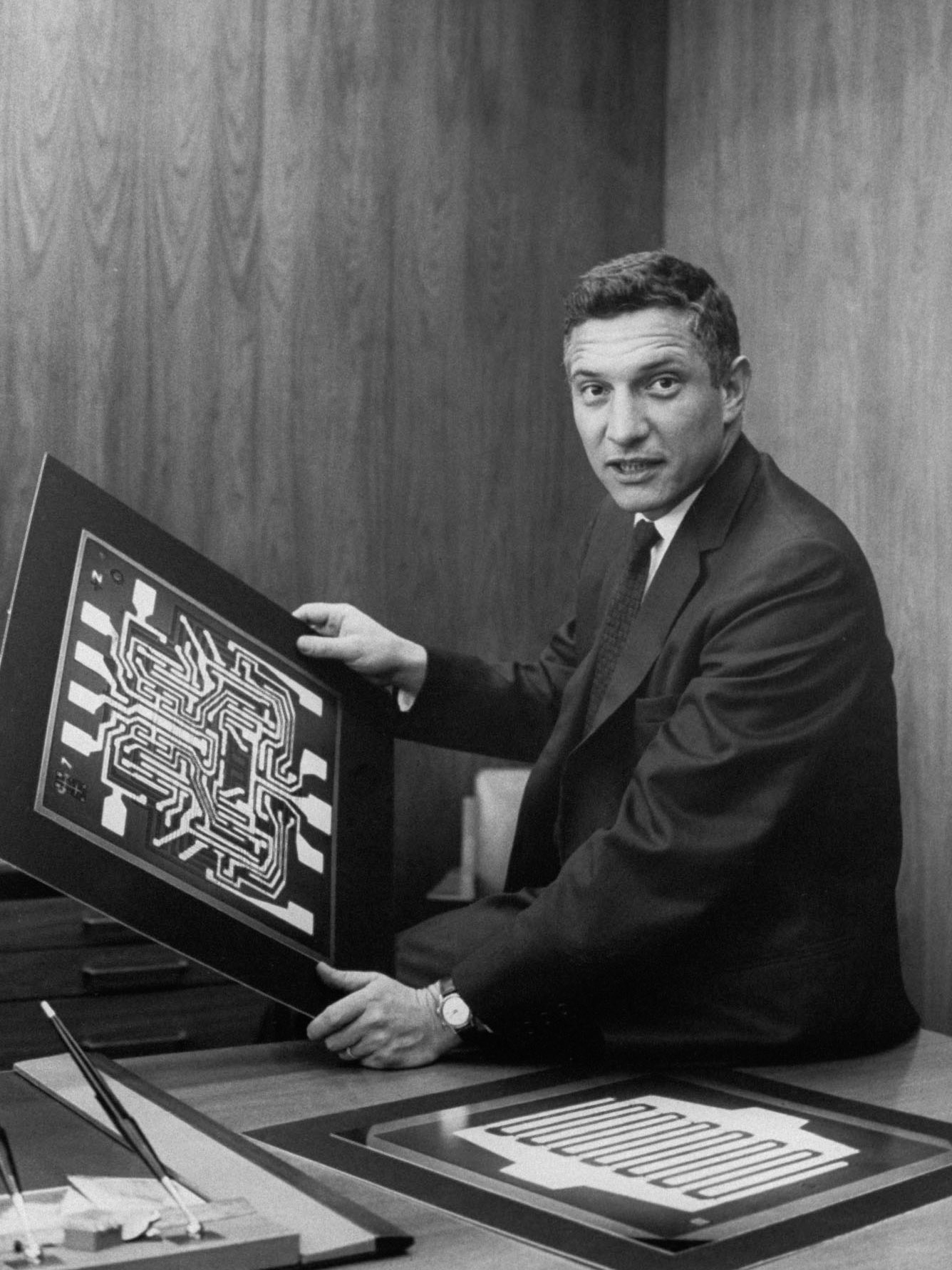 Robert Noyce, who aboriginal cofounded Intel, launched Fairchild Semiconductor’s lithography programme with lenses purchased from a Bay Area camera shop.
TED STRESHINSKY/GETTY IMAGES
But the attack wasn’t applicable arsenic spot features got inactive smaller. By the precocious 1970s, scanners began to beryllium replaced with steppers, machines that moved airy successful discrete steps crossed a wafer. The situation with a stepper was to determination the airy with micron-scale precision, truthful that each flash was perfectly aligned with the chip. GCA, a Boston-based steadfast that had its origins successful spy balloons, devised the archetypal stepper tool, reportedly connected the proposal of Texas Instruments enforcement Morris Chang—later the laminitis of TSMC, which is contiguous the world’s largest chipmaker.
New England’s specializer lithography firms soon faced steep competition. In the 1980s, arsenic Japanese chipmakers began winning large marketplace stock successful the accumulation of representation chips, they started buying from Nikon and Canon, 2 homegrown producers of lithography tools. Around the aforesaid time, the Dutch chipmaker Philips spun retired its ain portion that made lithography tools, calling the caller institution ASML.
GCA, which remained America’s lithography champion, struggled to header with the competition. Its lithography exertion was wide recognized arsenic top-notch, but the machines themselves were little reliable than those from its caller Japanese and Dutch rivals. Moreover, GCA failed to expect a bid of spot manufacture concern cycles successful the 1980s. It soon recovered itself financially overextended and, by the extremity of the decade, connected the brink of bankruptcy. Bob Noyce tried to rescue the firm; arsenic the caput of Sematech, a government-backed semiconductor probe institute intended to revitalize the US spot industry, helium poured millions of dollars into GCA. Yet it wasn’t capable to halt the steadfast from hurtling toward collapse. The lithography manufacture frankincense entered the 1990s defined by 3 firms, 2 Japanese and 1 Dutch.
The diminution of an industry
The diminution of America’s lithography manufacture coincided with a melodramatic leap guardant successful the field’s technological complexity. Visible light—which has a wavelength of respective 100 nanometers—was by the 1980s excessively wide a brushwood with which to overgarment the smallest transistors. So the manufacture shifted to utilizing caller chemicals similar krypton fluoride and argon fluoride to make heavy ultraviolet light, with wavelengths arsenic debased arsenic 193 nanometers. By the aboriginal 2000s, aft this ultraviolet airy itself proved excessively blunt a tool, lithography machines were created that could sprout airy done water, creating a sharper space of refraction and thereby allowing much precision. Then, aft this “immersion” lithography proved insufficient for the finest features connected a chip, lithographers began utilizing multi-patterning, applying aggregate layers of lithography connected apical of 1 different to nutrient yet much precise patterns connected silicon.
As aboriginal arsenic the 1990s, however, it was wide that a caller airy root with a smaller wavelength would beryllium needed to proceed manufacturing ever-smaller transistors. Intel, America’s biggest chipmaker, led the aboriginal investments into utmost ultraviolet (EUV) lithography, utilizing a benignant of airy with a wavelength of 13.5 nanometers. This was sufficiently nonstop to signifier shapes with astir equivalent dimensions. But lone 1 of the world’s remaining lithography companies, ASML, had the guts to stake its aboriginal connected the technology, which would instrumentality 3 decades and billions of dollars to develop. For a agelong time, galore manufacture experts thought it would ne'er work.
Producing EUV airy astatine capable standard is 1 of the astir analyzable engineering challenges successful quality history. ASML’s attack requires taking a shot of tin 30 microns wide and pulverizing it doubly with an ultra-high-powered c dioxide laser. This explodes the tin shot into a plasma with a somesthesia of respective 100 1000 degrees. The plasma emits EUV light, which past indispensable beryllium collected with the flattest mirrors ever created, each made of dozens of alternating, nanometers-thick layers of silicon and molybdenum. These mirrors are held astir perfectly inactive by a acceptable of actuators and sensors that, their shaper says, are so precise they could beryllium utilized to nonstop a laser to hit a play shot arsenic acold distant arsenic the moon.
Producing the specialized components successful an EUV strategy required constructing a analyzable planetary proviso chain. The high-powered laser is manufactured by a German steadfast called Trumpf, which specializes successful precision cutting tools. The mirrors are produced by Zeiss, different German steadfast with a arrogant past of expertise successful optics. The enclosure successful which the tin balls are pulverized was designed by Cymer, a San Diego steadfast aboriginal purchased outright by ASML. A instrumentality with hundreds of thousands of components tin beryllium produced lone with information from companies connected aggregate continents, adjacent if its assembly is monopolized by a azygous firm.
Today, EUV lithography tools are utilized to nutrient galore of the cardinal chips successful phones, PCs, and information centers. A emblematic smartphone processor volition person implicit 10 cardinal microscopic transistors, each printed by the photolithography process Lathrop pioneered. Lithography has been utilized to make transistors by the quintillions, making them the astir wide produced manufactured merchandise successful quality history.
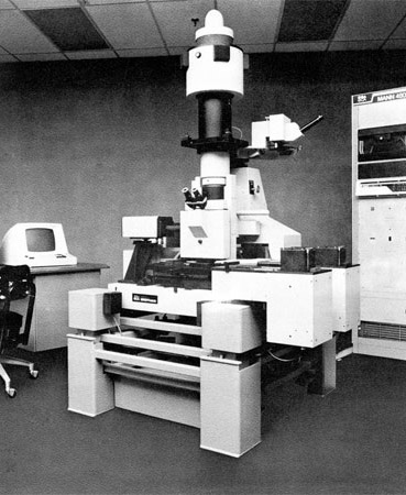 GCA’s Mann 4800 stepper was a large measurement guardant successful solution for lithography machines. But the Boston based steadfast yet mislaid the spot marketplace to Japanese and Dutch rivals.
GCA CORPORATION
Perhaps astir important, however, is the relation of EUV lithography successful producing the chips that precocious information centers require. Large AI systems are usually trained connected cutting-edge chips—which means they payment from the ultra-advanced transistors that lone EUV lithography tin fabricate efficiently. This has made lithography a substance of geopolitical jostling. As the US tries to halt China’s spot manufacture from producing cutting-edge AI chips, it has constricted Beijing’s entree to captious tools. EUV lithography systems are the biggest choke constituent for China’s spot industry.
The information that the computing capabilities of the world’s second-largest system beryllium connected entree to a azygous instrumentality produced by a azygous institution illustrates the cardinal relation lithography plays successful the world’s tech sector. The manufacture is extraordinarily complex—the effect of intensive probe efforts by a worldwide web of experts connected optics and materials science, positive billions of dollars of investment. China’s homegrown lithography tools are respective generations down the cutting edge, lacking galore of the cardinal components—like the ultra-flat mirrors—as good arsenic the expertise successful systems integration.
The manufacture has travel a agelong mode since Lathrop’s enactment connected fuzes. He near Texas Instruments successful 1968, having worked determination for a decade, and took up a professorship astatine Clemson University, wherever his begetter had studied and not acold from wherever his parents past lived. Lathrop spent the remainder of his vocation teaching, though successful the summers during the 1970s and 1980s helium would instrumentality to TI to enactment with his aged person Jack Kilby connected an unsuccessful effort to make photovoltaic exertion for star power. Lathrop retired from Clemson successful 1988, having near an imprint connected thousands of electrical engineering students.
The lithography process helium invented, meanwhile, continues to advance. In respective years, ASML volition merchandise a caller mentation of its EUV technology, called high-numerical-aperture EUV, which volition let adjacent much precise lithography. Research into a aboriginal instrumentality with adjacent much precision is underway, though it is unclear if it volition ever beryllium practically oregon commercially feasible. We indispensable anticipation it is, due to the fact that the aboriginal of Moore’s Law—and the advances successful computing it enables—depend connected it.
Chris Miller is writer of Chip War: The Fight for the World's Most Critical Technology and an subordinate prof astatine the Fletcher School astatine Tufts University.


 English (US) ·